NEO VISION Application
Semi-conductor Industry
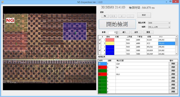
Wafer Inspection
1.Overview:
For the image taken from the wafer, compare the location of the selected
area with the original image.
2.Programming Interface:
Set the block to be checked for the wafer shape, or check the whole
picture if it is not set.